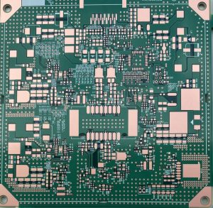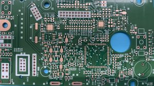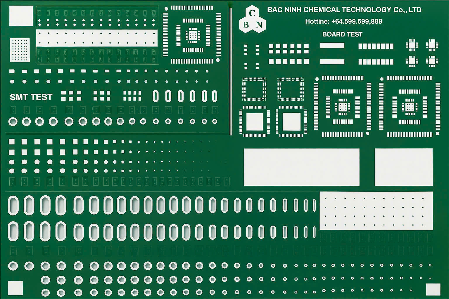



OSP in PCB manufacturing stands for Organic Solderability Preservative, a thin, flat protective coating made from organic compounds applied to the copper surface of printed circuit boards (PCBs) to prevent oxidation and corrosion before soldering. OSP is easily removed by flux before soldering, exposing the clean copper layer and allowing for high-quality solder joints.
Currently, there are two main organic coating systems: Imidazole and Benzimidazole.
The main roles and advantages of OSP:
- Copper surface protection: Prevents oxidation, maintains the copper in good conditions and ready for soldering.
- Flat surface: Provides an excellent flat surface, ideal for soldering small components and high-precision applications.
- Environmentally friendly: Lead-free, RoHS compliant, halogen-free, and uses a water-based chemical process.
- Low cost: The process is simple and takes less time, resulting in lower production costs.
The OSP treatment procedure:
1. Degreasing
This step is highly recommended, especially for circuit boards manufactured using the print-etch process, as there may be residual oil and grease from the board cutting process. For double-sided and multi-layer circuit boards, this step is also necessary because the Solder mask drying process can cause significant oxidation of the copper surface.
2. Water rinse
3 consecutive cascade rinse is to remove completely the remain degreasing chemical
3. Microetching
No special chemicals are required. For example, a 5% sulfuric acid solution is sufficient to remove residual impurities after microetching with SPS.
If a hydrogen peroxide base solution was used in the previous step, this acid rinse may not be necessary.
4. Water rinse
3 consecutive cascade rinse is to remove completely the drag-out solution from the Microetching step.
5. Acid rinse
No special chemicals are required. For example, a 5% sulfuric acid solution is sufficient to remove residual impurities after microetching with SPS.
If a hydrogen peroxide base solution was used in the previous step, this acid rinse may not be necessary.
6. Water rinse
3 consecutive cascade rinse is to remove completely the contaminations that can get into OSP solution.
The pH of the final rinse water bath should be measured to monitor the chemical dragged from previous treatment steps.
7. Air knife
Completely blow away any remaining water from the product, especially in the through-hole, to avoid contaminating the tin plating solution.
Hot air is not required—high-pressure dry air will suffice.
8. OSP
- Dipping at 40-45°C for 60-120 seconds is the standard condition to achieve optimal coating thickness.
- The pH and concentration of the active ingredient must be controlled within the standards according to the maintenance instructions of the OSP chemical being used.
- It is highly recommended to completely submerge the circuit board in the solution instead of using a spray method, to ensure that the OSP layer can evenly be applied even in the through-holes.
Additionally, spraying the solution from below using a pressurized jet nozzle can also improve performance
- OSP solution is ready to use and does not require dilution.
- The transfer roller should be designed with a lightweight shaft and be of the geared roller type.
- Absolutely do not use rubber materials such as EPDM for any part of the OSP system, as crystallization will make surface cleaning very difficult.
9. Squeezing rollers
- Using a roller is very helpful in minimizing the amount of OSP solution dragged out, and also helps form a more uniform and effective coating compared to using air knife.
- Rollers made from soft materials such as PP (polypropylene) or PVAc (polyvinyl acetate) in a porous (sponge) form are recommended.
- Using an air knife in conjunction with the roller is not recommended, as the roller will always be dried, causing the crystallization of active ingredient in the solution from the remaining drag-out. This makes the roller sticky, and in the worst case: the OSP coating may be peeled off from the circuit board surface due to sticking to the roller and then, that coating may be rolled onto other circuit boards.
10. Water rinse
3 consecutive cascade rinse with high flow rate.
DI water is strongly recommended to prevent Tin layer from ion contamination.
High pressure rinse helps take the remain chemical in through-hole out, specially small hole.
11. Drying
The product passes through a drying step at a temperature of 80-90 degrees Celsius for 30-45 seconds to completely dry the through-holes.