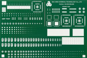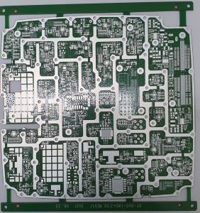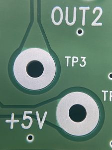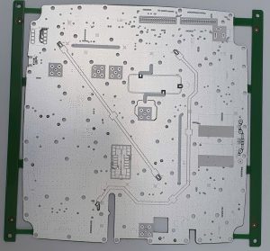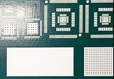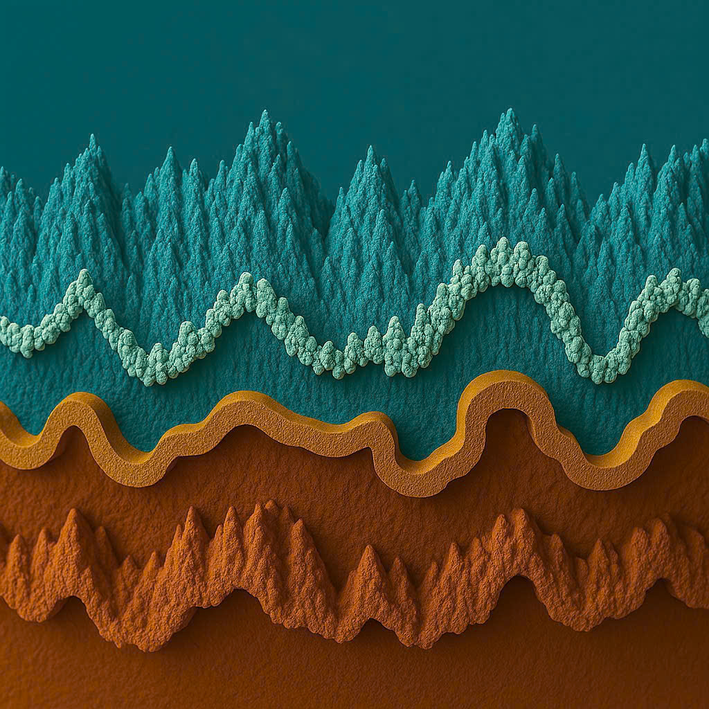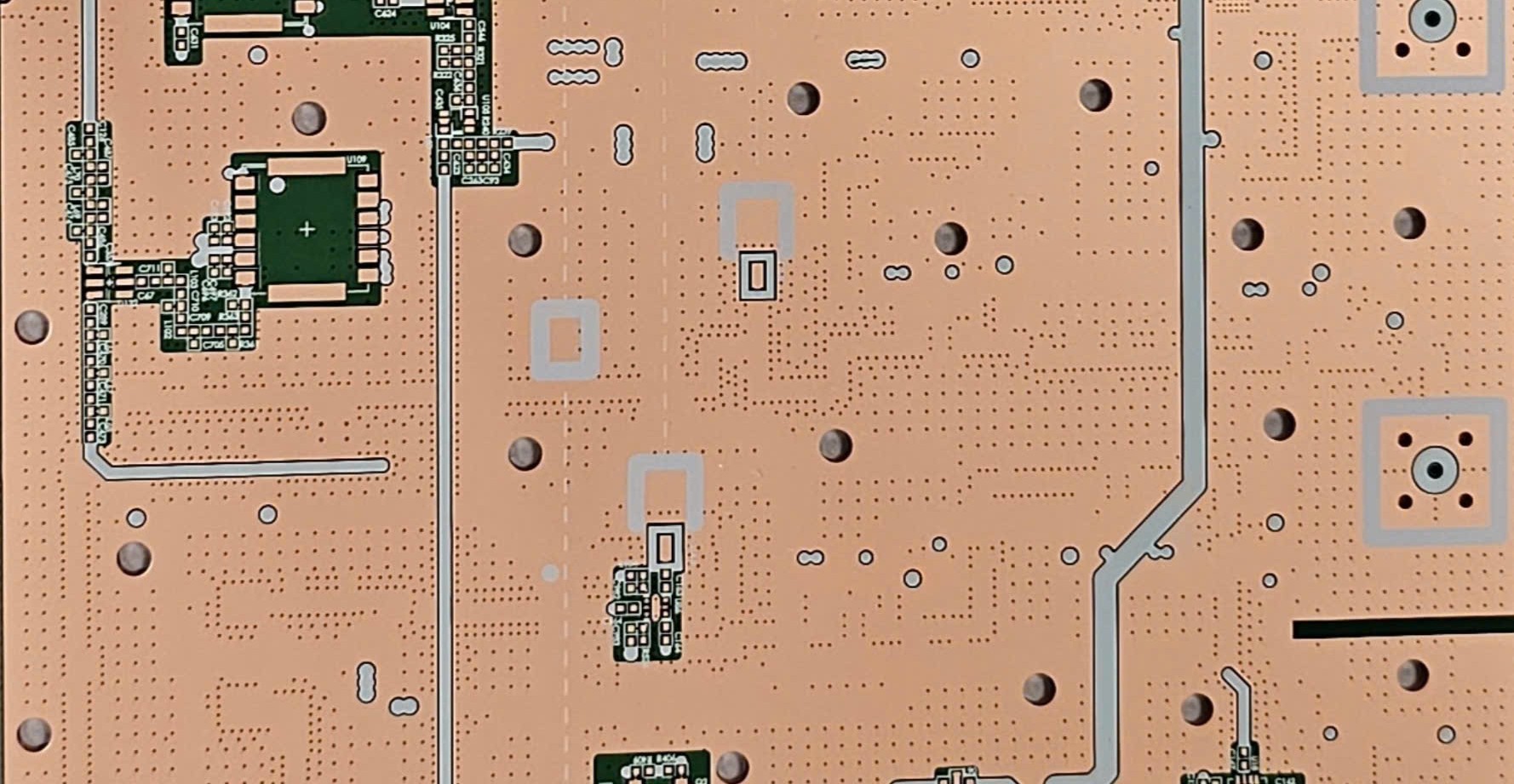



Immersion Tin is the final finishing step in the PCB manufacturing process before components are mounted onto the board. A Tin layer, with thickness from 0.5µm to 1.2µm, is applied over the copper substrate of the PCB. This method is a cost-effective solution for lead-free PCBs, resulting in a flat, consistent surface, good solderability, and high efficiency. The tin layer is typically white, hence the finish is sometimes called “white tin,” and it is applied to the copper using an non-electric chemical plating bath. This tin surface finish protects the underlying copper from oxidation throughout the PCB’s intended lifespan.
The Immersion Tin line include:
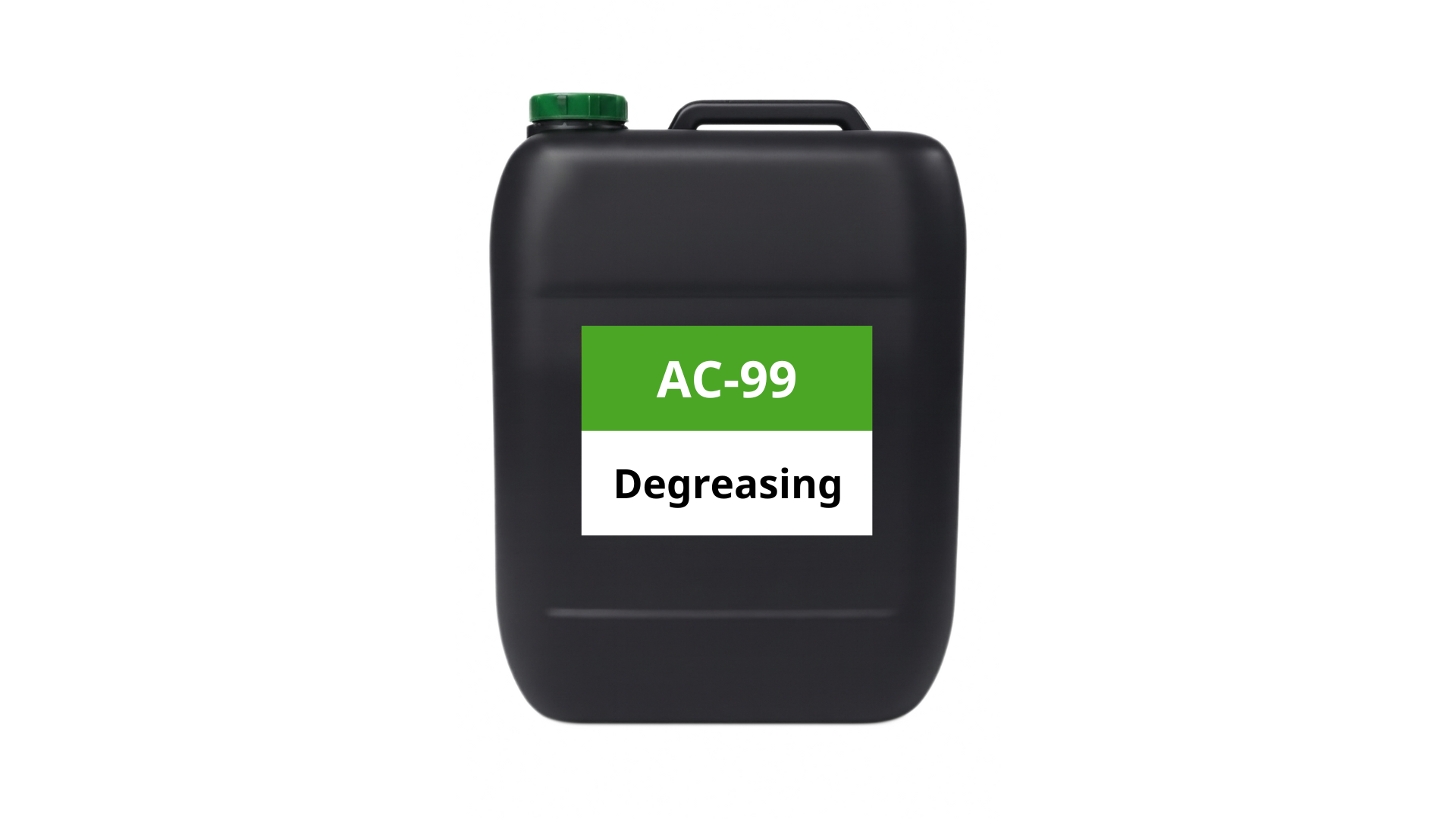
1. Degreasing
Degreasing is first step tht involves cleaning away organic impurities, grease stains, fingerprints, and copper oxides from the product surface.
Highly recommendable especially for print-etch boards due to oil residue by punching, but also for double sided and multilayer boards due to severe copper oxidation by curing for solder mask ink.
2. Water rinse
3 consecutive cascade rinse is to remove completely the remain degreasing chemical
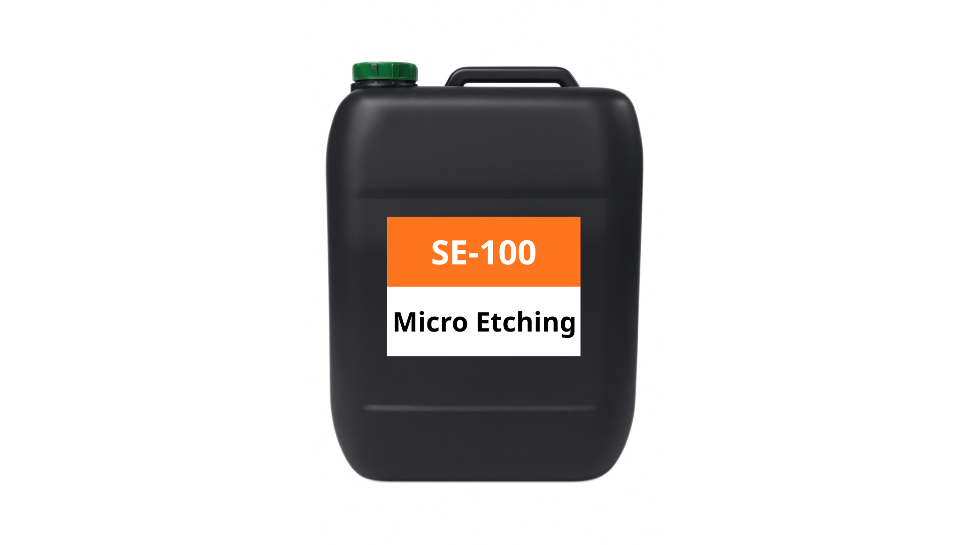
3. Microetching
A solution of H2SO4/H2O2 + surface treatment additives is the recommended choice, as it results in a better plating surface.
SPS (Sodium Persulfate – Na2S2O8) base solution can be used; however, an additional acid cleaning step is recommended afterward to remove chemical residue.
Maintain a minimum etching rate of 1.5 microns on the copper layer for optimal plating performance.
4. Water rinse
3 consecutive cascade rinse is to remove completely the drag-out solution from the Microetching step.
5. Acid rinse
No special chemicals are required. For example, a 5% sulfuric acid solution is sufficient to remove residual impurities after microetching with SPS.
If a hydrogen peroxide base solution was used in the previous step, this acid rinse may not be necessary.
6. Water rinse
3 consecutive cascade rinse is to remove completely the contaminations that can get into OSP solution.
The pH of the final rinse water bath should be measured to monitor the chemical dragged from previous treatment steps.
7. Air knife
Completely blow away any remaining water from the product, especially in the through-hole, to avoid contaminating the tin plating solution.
Hot air is not required—high-pressure dry air will suffice.
8. Tin Predip
Form a thin layer of tin to the product surface before increasing the tin thickness in the next step.
9. Tin chemical plating
Accelerate the tin plating reaction.
Temperature: 65 ~ 70°C
Achieved thickness: 0.5 ~ 1.2 µm depending on immersion time.
10. Water rinse
3 consecutive cascade rinse with high flow rate.
DI water is strongly recommended to prevent Tin layer from ion contamination.
High pressure rinse helps take the remain chemical in through-hole out, specially small hole.
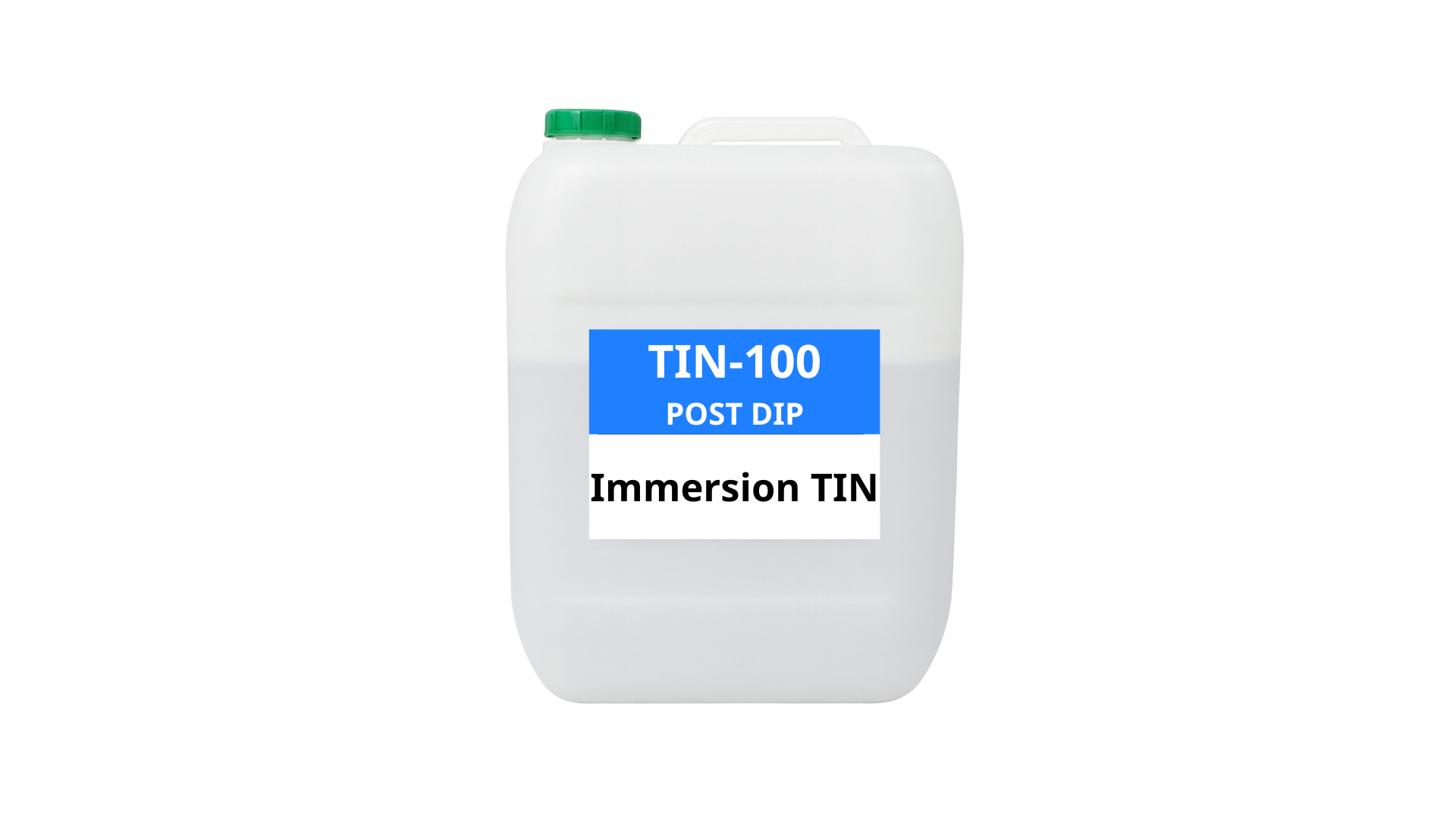
11. Post Dip
The antioxidized chemical protects Tin surface for longer time.
12. Water rinse
3 consecutive cascade rinse with high flow rate to take the remain chemical in through-hole and on surface out.
13. Air Knife
Remove the remain water on surface and in hole
Above 5KPa air pressure is recommended for better removal performance.
14. Drying
The product passes through a drying step at a temperature of 80-90 degrees Celsius for 60-90 seconds to completely dry the through-holes, preventing any remaining moisture inside the holes from causing oxidation of the tin surface later on.